Welcome to our site! EDAboard.com is an international Electronics Discussion Forum focused on EDA software, circuits, schematics, books, theory, papers, asic, pld, 8051, DSP, Network, RF, Analog Design, PCB, Service Manuals... and a whole lot more! To participate you need to register. Registration is free. Click here to register now.
Currently, I am engaged in the design of a Thermal Shutdown circuit for an LDO regulator. In this endeavor, I have obtained a circuit schematic from a senior colleague, which utilizes three NMOS transistors configured as voltage dividers.
This particular arrangement is employed due to the...
Thank you all for all the information and suggestion. Indeed as pointed by FvM and KlausST, the problem is with 0 voltage applied at the gate of the input transistors for which the gain drops and falls between 0 and 1, thus giving a negative loop gain. I have also tried the Middlebrooks's...
Thank you sir for the insight. I have attached the image for loop gain setup as you recommended. I guess it is a correct setup and the system is fairly unstable due to a very low frequency pole. I will look into the stability matter. However sir I had a question as how the negative gain is...
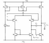
I am trying to design an LDO with the following specification: Vout = 1.5V; Vin = 1.7V - 2V; Iload = 75uA to 1200uA. However, while I am simulating its loop gain, its gain is coming negative. Even though all the transistors are in saturation within the given load condition. I have attached the...
I am recently studying "Analysis and Design of Analog IC" by Gray, Hurst, Lewis & Meyer. In chapter 6, pg 428 for a design of a classical 2stage op-amp having PMOS differential inputs, there is a statement: "In MOS technologies, however, the gm*ro (intrinsic gain), the product is usually between...
This site uses cookies to help personalise content, tailor your experience and to keep you logged in if you register.
By continuing to use this site, you are consenting to our use of cookies.